Ode to (Gordon) Moore’s Law
Monday, February 6th, 2023Chip War, The Fight For the World’s Most Critical Technology, 2022, Christopher Miller

This reader is a retired software engineer whose 40 year career began with punch card mainframes and ended with microcontrollers with embedded graphic displays, WiFi, and flash memory on a single chip. My introduction to computing was as a graduate research assistant on an ARPA funded project to study the dimensionality of nations. Since that time I followed the development of the ARPANET. I have lived the profound impact of Moore’s Law, needing to constantly anticipate where technology would be when project development required several years before introduction. Moore’s Law has still not been broken after all these years.
To get some sense of what exponental increase in transistors looks like consider the 1980s Cray 2 supercomputer which was export restricted for national security reasons. The CRAY-2 stood nearly 4 feet tall with a 5.5-foot diameter and weighed 5,500 pounds. The iPhone 12 is 5,000 times faster than the Cray-2!
Exponential growth of a technology is unique in human history.
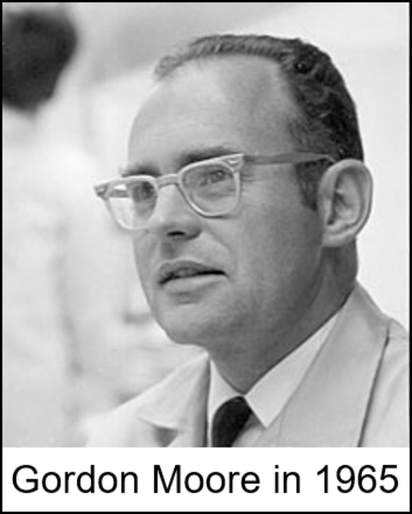
If the computing power on each chip continued to grow exponentially, Moore realized, the integrated circuit would revolutionize society far beyond rockets and radars…At Fairchild, Noyce and Moore were already dreaming of personal computers and mobile phones.
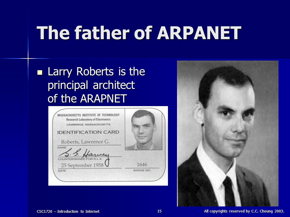
Alongside the rise of these new industrial titans (Intel and Micron), a new set of scientists were preparing a leap forward in chipmaking and devising revolutionary new ways to use processing power. Many of these developments occurred in coordination with government efforts, usually not the heavy hand of Congress or the White House, but the work of small, nimble organizations like DARPA (originally ARPA, Larry Robert director 1966-1973) that were empowered to take big bets on futuristic technologies — and to build the educational and R&D infrastructure that such gambles required.
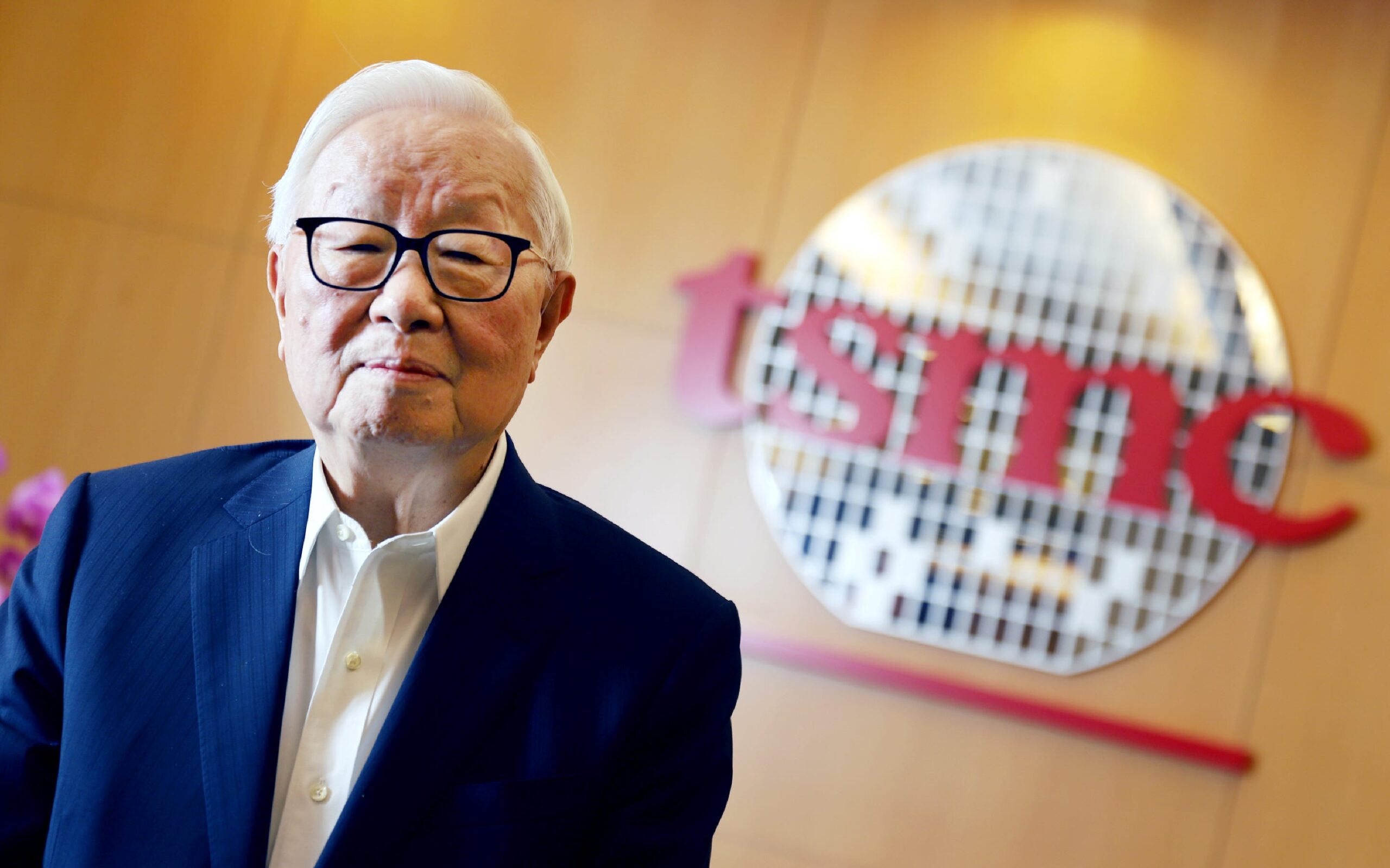
Morris Chang Founder of TSMC
(Dutch) ASML‘s history of being spun out of Philips helped in a surprising way, too facilitating a deep relationship with Taiwan’s TSMC (founder Morris Chang). Philips had been the cornerstone investor in TSMC, transferring its manufacturing process technology and intellectual property to the young foundry. This gave ASML a built-in market, because TSMC’s fabs were designed around Philip’s manufacturing processes. An accidental fire in TSMC’s fab in 1989 helped too, causing TSMC to buy additional nineteen new lithography machines, paid for by the fire insurance. Both ASML and TSMC started as small firms on the periphery of the chip industry, but they grew together, forming a partnership without which advances in computing today would have ground to a halt.
The next generation EUV (Extreme ultraviolet) lithography would therefore be mostly assembled abroad, though some components continued to be built in facility in Connecticut. Anyone who raised the question of how the U.S. would guarantee access to EUV tools was accused of retaining a Cold War mindset in a globalizing world. Yet the business gurus who spoke about technology spreading globally misrepresented the dynamic at play. The scientific networks that produced EUV spanned the world, bringing together scientists from countries as diverse as America, Japan, Slovenia, ad Greece. However, the manufacturing of EUV wasn’t globalized, it was monopolized. A single supply chain managed by a single company would control the future of lithography.
By the mid 2000’s, just as cloud computing was emerging, Intel had won a near monopoly over data center chips, competing only with AMD. Today nearly every major data center uses X86 chips from either Intel or AMD. The cloud can’t function without their processors… Some companies tried challenging z86’s position as the industry standard in PCs. In 1990 Apple and two partners established a joint venture called Arm, based in Cambridge England. The aim was to design processor chips using a new instruction set architecture based on the simpler RISC (reduced instruction set computer) principles that Intel had considered but rejected. As a startup Arm faced no costs of shifting away from x86, because it had no business and no customers. Instead, it wanted to replace X86 at the center of the computing ecosystem. Arm’s first CEO, Robin Saxby, had vast ambitions for the twelve-person startup…However Aim failed to win market share in PC’s in the 1990s and 2000’s, because Intel’s partnership with Microsoft’s Windows operating system was simply too strong to challenge. However Arm’s simplified, energy-efficient architecture quickly became popular in small, portable devices that had to economize on battery use. Nintendo chose Arm based chips for its handheld video games…
The problem wasn’t that no one realized Intel ought to consider new products, but that the status quo was simply too profitable. If Intel did nothing at all it would still own two of the world’s most valuable castles–PC and server chips–surrounded by a deep x86 moat.
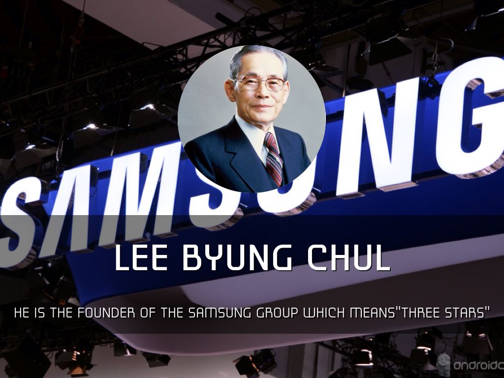
Intel turned down the iPhone contract…Apple looked elsewhere for its phone chips. Jobs turn to Arm’s architecture, which, unlike the x86 was optimized for mobile devices that had to economize on power consumption. The early iPhone processors were produced by Samsung (founder Lee Byung-chul), which had followed TSMC into the foundry business… By the time Otellini (Intel) realized his mistake, however it was too late.
By the 2000’s, it was common to split the semiconductor industry into three categories. “Logic” refers to the processors that run smartphones, computers, and servers. “Memory” refers to DRAM which provides the short-term memory computers need to operate, and flash, also called NAND, which remembers data over time. The third category of chips is more diffuse, including analog chips like sensors that convert visual or audio signals into digital data, radio frequency chips that communicate with cell phone networks, and semiconductors that manage how devices use electricity.
It (America’s second class status) dates to the late 1980s when Japan first overtook the U.S. DRAM output. The big shift in recent years is the collapse in the share of logic chips produced in the United States. Today, building an advanced logic fab costs $20 billion, an enormous capital investment that few firms can afford…Given the benefits of scale, the number of firms fabrication advanced logic chips has shrunk relentlessly.

Jensen Huang CEO Nvidia
Nvidia (which became dominant in graphics) not only designed chips called graphic processors units (GPUs) capable of handling 3D graphics, it also devised a software ecosystem around them. Making realistic graphics requires use of programs called shaders, which tell all the pixels in a image how they should be portrayed in, say a given shade of light. The shader is applied to each of the pixels in a image, a relatively straightforward calculation conducted over many thousands of pixels. Nvidia’s GPUs can render images quickly because, unlike Intel’s microprocessors or other general-purpose CPUs, they’re structured to conduct lots of simple calculations–like shading pixels–simultaneously.
In 2006, realizing that high-speed parallel computations could be used for purposes besides computer graphic, Nvidia released CUDA, software that lets GPUs be programmed in a standard programming language, without any reference to graphic at all. Even as Nvidia was churning out top-notch graphic chips, Huang (CEO) spent lavishly on this software effort, at least $10 billion,…to let any programmer–not just graphic experts–work with Nvidias chips…Nvidia discovered a vast new market for parallel processing, from computational chemistry to weather forecasting. At the time, Huang could only dimly perceive the potential growth in what would become the biggest use case for parallel processing, artificial intelligence.
Today Nvidia’s chips, largely manufactured by TSMC, are found in most advanced data centers.

Dr. Irwin Jacobs co founder Qualcom
For each generation of cell phone technology after 2G, Qualcomm contributed key ideas about how to transmit more data in the radio spectrum and sold specialized chips with the computing power capable of deciphering this cacophony of signals. The companies patents are so fundamental it’s impossible to make a cell phone without them. Qualcomm soon diversified into a new business line, designing not only the modem chips in a phone that communicate with a cell network, but also the application processors that run a smartphone’s core systems. These chip designs are monumental engineering accomplishments, each built on tens of millions of lines of code.
For many years, each generation of manufacturing technology was named after the length of the transistor’s gate, the part of the silicon chip whose conductivity would be turned on and off, creating and interrupting the circuit. The 180nm node was pioneered in 1999, followed by 130nm, 90nm, 65nm, and 45nm, with each generation shrinking transistors enough to make it possible to cram roughly twice as many in the same area. This reduced power consumption per transistor, because smaller transistors needed fewer electrons to flow through them.
Around the early 2010s, it became unfeasible to pack transistors more densely by shrinking them two dimensionally. One challenge was that, as transistors were shrunk according to Moore’s Law, the narrow length of the conductor channel occasionally caused power to “leak” through the circuit even when the switch was off. On top of this, the layer of silicon dioxide atop each transistor became so thin that quantum effects like “tunneling”–jumping through barriers that classical physics said should be insurmountable–began seriously impacting transistor performance. By the mid 2000s. the layer of silicon dioxide on top of each transistor was only a couple of atoms thick, too small to keep a lid on all the electrons sitting in the silicon.
To better control the movement of electrons, new materials and transistor designs were needed. Unlike the 2D design used sine the 1960s, the 22nm node introduced a new 3D transistor, called a FinFET (pronounced finfet), that sets the two ends of the circuit and the channel of semiconductor material that connects them on top of a block, looking like a fin protruding from a whale’s back. The channel that connects the two ends of the circuit can therefore have an electric field applied not only from the top but also from the sides of the fin, enhancing control over the electrons and overcoming the electricity leakage that was threatening the performance of new generations of tiny transistors…These nanometer-scale 3D structures were crucial for the survival of Moore’s Law, but they were staggeringly difficult to make, requiring even more precision in deposition, etching, and lithography. This added uncertainty about whether the major chip-makers would all flawlessly execute the switch to FinFET architectures or whether one might fall behind…Moreover, the 2008-2009 financial crisis was threatening to reorder the chip industry. Consumers stopped buying electronics, so tech firms stopped ordering chips.
Smartphones and PCs are both assembled largely in China with high-value components mostly designed in the U.S., Europe, Japan, or Korea. For PCs, most processors come from Intel and are produced at one of the company’s fabs in the U.S., Ireland, or Israel. Smartphones are different. They are stuffed full of chips, not only the main processor (which Apple designs itself), but modem and radio frequency chips for connecting with cellular networks, chips for WiFi and Bluetooth connections, an image sensor for the camera, at least two memory chips, chips that sense motion (so your phone knows when you turn it horizontal), as well as semiconductors that manage the battery, the audio, the wireless charging. These chips make up most of the bill of materials needed to build a smartphone.
As semiconductor fabrication capacity migrated to Taiwan and South Korea, so too did the ability to produce many of these chips. Application processors, the electronic brain inside each smartphone, are mostly produced in Taiwan and South Korea before being sent to China for final assembly inside a phones plastic case and glass screen. Apple’s iPhone processors are fabricated exclusively in Taiwan.
These tricks kept Moore’s Law alive, as the chip industry shrank transistors from the 180nm node in the late 1990s, through the early stages of 3D FinFET chips, which were ready for high-volume manufacturing by the mid-2010s.
However, there were only so many optical tricks that could help 193nm light carve smaller features. Each new workaround added time and cost money. By the mid-2010s, it might have been possible to eke out a couple of additional improvement, but Moore’s Law needed better lithography tools to carve smaller shapes. The only hope was that the hugely delayed EUV lithography tools, which had been in development since the early 1990s, could finally be made to work at a commercial scale.
Even the deep pockets of the Persian Gulf royals who owned GlobalFoundries weren’t deep enough. The number of companies capable of fabricating leading-edge (7nm) chips fell from four to three. (TSMC, Intel, and Samsung).
As investors bet that data centers will require ever more GPUs, Nvidia has become America’s most valuable semiconductor company. Its assent isn’t assured however, because in addition to buying Nvidia chips the big cloud companies — Google, Amazon, Microsoft, Facebook, Tencent, Alibaba, and others — have also begun designing their own chips, specialized to their processing needs, with a focus on artificial intelligence and machine learning.
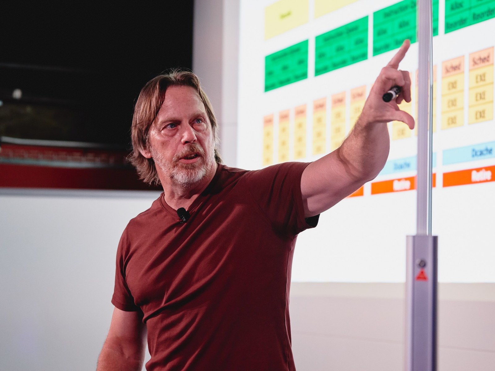
Master Chip Designer Jim Keller
Gordon Moore’s famous law is only a prediction, not a fact of physics…At some point, the laws of physics will make it impossible to shrink transistors further. Even before then, it could become too costly to manufacture them. The rate of cost declines has already significantly slowed. The tools needed to make ever-smaller chips are staggeringly expensive, none more so than the EUV lithography machines that cost more than $100 million each.
The end of Moore’s Law would be devastating for the semiconductor industry — and for the world. We produce more transistors each year only because it’s economically viable to do so.
The durability of Moore’s Law, in other words has surpassed even the person who it’s named after and the person who coined it. It may well surprise today’s pessimists too. Jim Keller, the star semiconductor designer who is widely credited for transformative work on chips at Apple, Tesla, AMD, and Intel has said he sees a clear path toward a fifty times increase in the density with which transistors can be packed on chips.”we’re not running out of atoms”, Keller has said. “We know how to print single layers of atoms.”